- 您现在的位置:买卖IC网 > Sheet目录3872 > PIC18F4450T-I/ML (Microchip Technology)IC PIC MCU FLASH 8KX16 44QFN
dsPIC30F3010/3011
DS70141F-page 46
2010 Microchip Technology Inc.
5.1
Interrupt Priority
The user-assignable Interrupt Priority (IP<2:0>) bits for
each individual interrupt source are located in the
3 LSbs of each nibble, within the IPCx register(s). Bit
3 of each nibble is not used and is read as a ‘0’. These
bits define the priority level assigned to a particular
interrupt by the user.
Since more than one interrupt request source may be
assigned to a specific user-assigned priority level, a
means is provided to assign priority within a given level.
This method is called “Natural Order Priority”.
Natural Order Priority is determined by the position of
an interrupt in the vector table, and only affects
interrupt operation when multiple interrupts with the
same user-assigned priority become pending at the
same time.
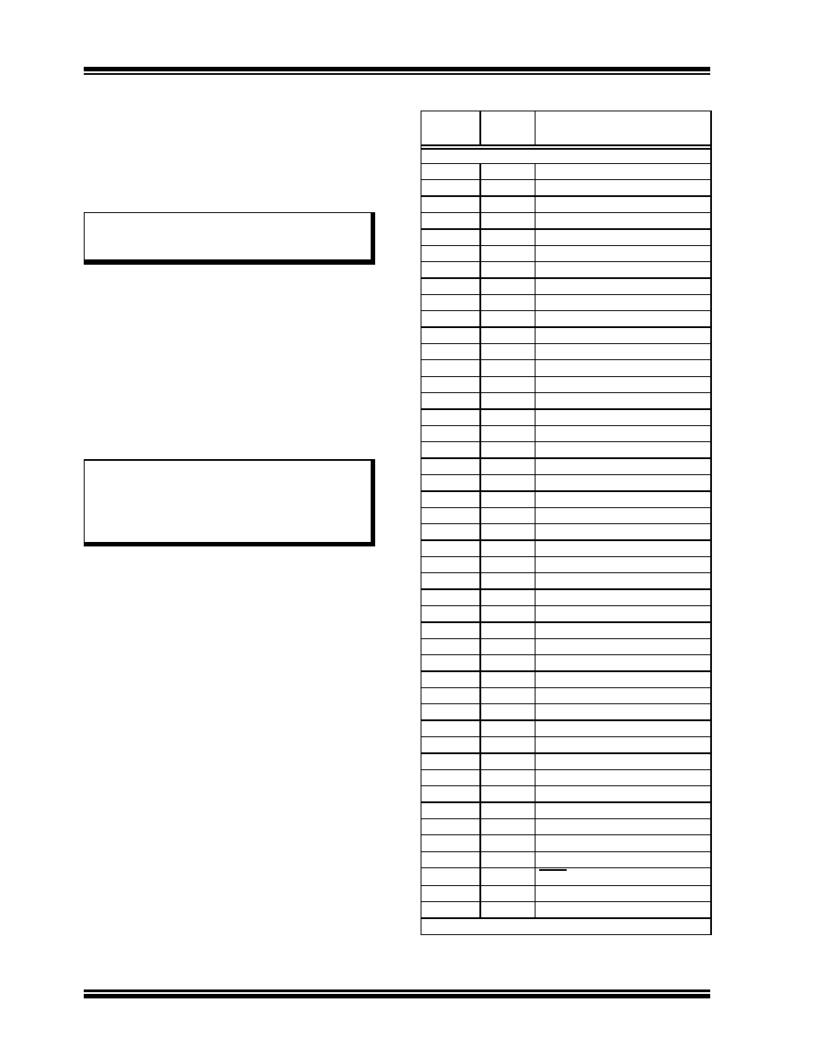
Table 5-1 lists the interrupt numbers and interrupt
sources for the dsPIC DSC devices and their
associated vector numbers.
The ability for the user to assign every interrupt to one
of seven priority levels implies that the user can assign
a very high overall priority level to an interrupt with a
low natural order priority. For example, the PWM Fault
A Interrupt can be given a priority of 7. The INT0
(external interrupt 0) may be assigned to priority
Level 1, thus giving it a very low effective priority.
TABLE 5-1:
INTERRUPT VECTOR TABLE
Note:
The user-assignable priority levels start at
0, as the lowest priority, and Level 7, as
the highest priority.
Note 1: The natural order priority scheme has 0
as the highest priority and 53 as the
lowest priority.
2:The natural order priority number is the
same as the INT number.
Interrupt
Number
Vector
Number
Interrupt Source
Highest Natural Order Priority
0
8
INT0 – External Interrupt 0
1
9
IC1 – Input Capture 1
2
10
OC1 – Output Compare 1
3
11
T1 – Timer1
4
12
IC2 – Input Capture 2
5
13
OC2 – Output Compare 2
6
14
T2 – Timer2
7
15
T3 – Timer3
8
16
SPI1
9
17
U1RX – UART1 Receiver
10
18
U1TX – UART1 Transmitter
11
19
ADC – ADC Convert Done
12
20
NVM – NVM Write Complete
13
21
SI2C – I2C Slave Interrupt
14
22
MI2C – I2C Master Interrupt
15
23
Input Change Interrupt
16
24
INT1 – External Interrupt 1
17
25
IC7 – Input Capture 7
18
26
IC8 – Input Capture 8
19
27
OC3 – Output Compare 3(1)
20
28
OC4 – Output Compare 4(1)
21
29
T4 – Timer4
22
30
T5 – Timer5
23
31
INT2 – External Interrupt 2
24
32
U2RX – UART2 Receiver(1)
25
33
U2TX – UART2 Transmitter(1)
26
34
Reserved
27
35
Reserved
28
36
Reserved
29
37
Reserved
30
38
Reserved
31
39
Reserved
32
40
Reserved
33
41
Reserved
34
42
Reserved
35
43
Reserved
36
44
Reserved
37
45
Reserved
38
46
Reserved
39
47
PWM – PWM Period Match
40
48
QEI – QEI Interrupt
41
49
Reserved
42
50
Reserved
43
51
FLTA – PWM Fault A
44
52
Reserved
45-53
53-61
Reserved
Lowest Natural Order Priority
Note 1:
Available on dsPIC30F3011 only
发布紧急采购,3分钟左右您将得到回复。
相关PDF资料
PIC18F4321T-I/ML
IC PIC MCU FLASH 4KX16 44QFN
PIC18F4221T-I/ML
IC PIC MCU FLASH 2KX16 44QFN
PIC18F2321T-I/ML
IC PIC MCU FLASH 4KX16 28QFN
PIC18F2221T-I/SO
IC PIC MCU FLASH 2KX16 28SOIC
PIC16LF1939-I/MV
IC MCU 8BIT 28KB FLASH 40-UQFN
PIC24F16KL402-I/SP
IC MCU 16BIT 16KB FLASH 28-SPDIP
PIC18F24J11-I/SS
IC PIC MCU FLASH 16K 2V 28-SSOP
PIC24F16KA101-I/SO
IC PIC MCU FLASH 16K 20-SOIC
相关代理商/技术参数
PIC18F4450T-I/PT
功能描述:8位微控制器 -MCU 16KB FL 768 RAM 34 I/O FS-USB 2.0 RoHS:否 制造商:Silicon Labs 核心:8051 处理器系列:C8051F39x 数据总线宽度:8 bit 最大时钟频率:50 MHz 程序存储器大小:16 KB 数据 RAM 大小:1 KB 片上 ADC:Yes 工作电源电压:1.8 V to 3.6 V 工作温度范围:- 40 C to + 105 C 封装 / 箱体:QFN-20 安装风格:SMD/SMT
PIC18F4455-BL
制造商:POWERLITE SYSTEMS 功能描述:PIC18F445 W/ BOOTLOADER FOR FLASHLAB 制造商:POWERLITE SYSTEMS 功能描述:PIC18F445 W/ BOOTLOADER, FOR FLASHLAB 制造商:POWERLITE SYSTEMS 功能描述:PIC18F445 W/ BOOTLOADER, FOR FLASHLAB; Silicon Manufacturer:Powerlite Systems; Core Architecture:PIC; Kit Contents:Board; Features:Bootloader Programming, RS232 Connector for Boot-Loading and Serial Comms ;RoHS Compliant: Yes
PIC18F4455-I/ML
功能描述:8位微控制器 -MCU 24kBF 2048RM FSUSB2 RoHS:否 制造商:Silicon Labs 核心:8051 处理器系列:C8051F39x 数据总线宽度:8 bit 最大时钟频率:50 MHz 程序存储器大小:16 KB 数据 RAM 大小:1 KB 片上 ADC:Yes 工作电源电压:1.8 V to 3.6 V 工作温度范围:- 40 C to + 105 C 封装 / 箱体:QFN-20 安装风格:SMD/SMT
PIC18F4455-I/P
功能描述:8位微控制器 -MCU 24kBF 2048RM FSUSB2 RoHS:否 制造商:Silicon Labs 核心:8051 处理器系列:C8051F39x 数据总线宽度:8 bit 最大时钟频率:50 MHz 程序存储器大小:16 KB 数据 RAM 大小:1 KB 片上 ADC:Yes 工作电源电压:1.8 V to 3.6 V 工作温度范围:- 40 C to + 105 C 封装 / 箱体:QFN-20 安装风格:SMD/SMT
PIC18F4455-I/PT
功能描述:8位微控制器 -MCU 24kBF 2048RM FSUSB2 RoHS:否 制造商:Silicon Labs 核心:8051 处理器系列:C8051F39x 数据总线宽度:8 bit 最大时钟频率:50 MHz 程序存储器大小:16 KB 数据 RAM 大小:1 KB 片上 ADC:Yes 工作电源电压:1.8 V to 3.6 V 工作温度范围:- 40 C to + 105 C 封装 / 箱体:QFN-20 安装风格:SMD/SMT
PIC18F4455T-I/ML
功能描述:8位微控制器 -MCU 24kBF 2048RM FSUSB2 RoHS:否 制造商:Silicon Labs 核心:8051 处理器系列:C8051F39x 数据总线宽度:8 bit 最大时钟频率:50 MHz 程序存储器大小:16 KB 数据 RAM 大小:1 KB 片上 ADC:Yes 工作电源电压:1.8 V to 3.6 V 工作温度范围:- 40 C to + 105 C 封装 / 箱体:QFN-20 安装风格:SMD/SMT
PIC18F4455T-I/PT
功能描述:8位微控制器 -MCU 24kBF 2048RM FSUSB2 RoHS:否 制造商:Silicon Labs 核心:8051 处理器系列:C8051F39x 数据总线宽度:8 bit 最大时钟频率:50 MHz 程序存储器大小:16 KB 数据 RAM 大小:1 KB 片上 ADC:Yes 工作电源电压:1.8 V to 3.6 V 工作温度范围:- 40 C to + 105 C 封装 / 箱体:QFN-20 安装风格:SMD/SMT
PIC18F4458-I/ML
功能描述:8位微控制器 -MCU 24KB Flash 2KB RAM RoHS:否 制造商:Silicon Labs 核心:8051 处理器系列:C8051F39x 数据总线宽度:8 bit 最大时钟频率:50 MHz 程序存储器大小:16 KB 数据 RAM 大小:1 KB 片上 ADC:Yes 工作电源电压:1.8 V to 3.6 V 工作温度范围:- 40 C to + 105 C 封装 / 箱体:QFN-20 安装风格:SMD/SMT